


Professional Development Courses
ESTC 2022 offers high-level Professional Development Courses on Tuesday, September 13th, in the morning. Don't miss this excellent opportunity to benefit from the knowledge of international electronic packaging expert.
Attending a PDC is possible for an additional fee. This fee includes course materials, coffee break and lunch after the PDC.
Please select the course you are interested in during your regular conference registration.
PDC A - Why is now the right time to start digitalizing electronics manufacturing with an end-to-end holistic solution?
Content
In this course, we will explore the key global trends impacting the Electronics Manufacturing and PCB Assembly Industry and the challenges that they bring to manufacturers – including the global shortage in components, dramatic increase in PCB complexity, significant increase in New Product Introductions (NPIs) and Product Revisions and decrease in lot sizes up to “lot-size-one”. We will demonstrate why digitalization of the electronics factory is the most effective solution to many of these challenges and why building a holistic end-to-end digitalization strategy can provide the most significant return-on-investment (ROI).
The PDC will also cover the topics, which have been described in the following e-book, white papers and webinar sessions:
- Siemens_ebook_Oren Manor_Advanced-Manufacturing-In-the-Digital-Age-2nd-edition_tcm27-97004.pdf
- Siemens-SW-(Mike Santarini)-Digital-transformation-How-Siemens-EDA-helps-you-engineer-a-smarter-future-faster-83731-WP-C5.pdf
- Siemens-PLM-Smart-manufacturing-for-electronics-WhitePaper_tcm27-57766.pdf
- Siemens-SW-A-comprehensive-digital-twin-for-PCB-assembly_WhitePaper_tcm27-64886.pdf
- Digital twin webinar series _ Jay Gorajia.docx
- Siemens-SW-Driving-engineering-for-vehicle-electrification-WhitePaper_tcm27-93397.pdf
Instructor

OREN MANOR, Siemens Digital Industries Software, Tel Aviv, Israel, holds a B.Sc. in Computer Science and Economics from Tel-Aviv University. He has been the Siemens Opcenter Core Business Director at Siemens Digital Industries Software since October 2021, where he manages the overall business strategy for the Digital Manufacturing portfolio for the Medical, Electronics and Semiconductors Industries. Before this he was Electronics Manufacturing Business Director at Mentor Graphics’ Valor Division. Oren Manor joined the Valor Division of Mentor Graphics in 2012 and served in a number of key business positions including Partner Management and Manufacturing Engineering Business Development. He previously served as VP of Sales and Marketing at Signature-IT, a software company providing data management solutions for industrial companies, and held senior sales and marketing positions at Jungo – a NDS company. After living in Stockholm, London, Philadelphia and Chicago, Oren resides in Tel Aviv. He is passionate about technology and an evangelist for automating electronics manufacturing; expert in Electronics, Medical, Semiconductor and discrete manufacturing; frequent speaker at leading industry and Siemens Software events. He has extensive Business Development experience in building comprehensive go-to-market strategies for Enterprise and B2B software applications.
PDC B - Advances in Fan-Out Wafer Level Packaging (FOWLP)
Content
After scale-up and high-volume manufacture of simple single-chip Fan-Out Wafer Level Packaging (FO-WLP) solutions by companies like Qualcomm and Infineon, now many premier semiconductor companies and OEM’s have adopted Advanced Fan-Out structures including Apple, AMD, MediaTek, HiSilicon, and Xilinx. These companies are leveraging foundry technologies like InFO offered by TSMC as well as OSAT solutions from ASE, Amkor, SPIL, PTI, DECA, and Nepes. This course will cover the advantages of FO-WLP, potential application spaces, advanced package structures available in the industry, technology roadmaps, and benchmarking. The challenges of moving from 300mm FO-WLP to panel will also be discussed.
Course Outline:
- Definitions and Advantages
- Advanced Applications
- Package Structures including Advanced FO technologies
- Technology Roadmap
- Panel Challenges
- Benchmarking
Instructor

BETH KESER, Ph.D., Intel, a recognized global leader in the semiconductor packaging industry with over 23 years of experience, received her B.S. degree in Materials Science and Engineering from Cornell University and her Ph.D. from the University of Illinois at Urbana-Champaign. Beth’s excellence in developing revolutionary electronic packages for semiconductor devices has resulted in 41 patents and patents pending and over 50 publications in the semiconductor industry. Previously, Beth led Qualcomm’s Fan-Out and Fan-In Wafer Level Packaging Technology Development and NPI Group for over 7 years where her team qualified over 50 products resulting in over 7 billion units shipped. In 2019, Beth published Advances in Embedded and Fan-Out Wafer-Level Packaging Technologies (Wiley) and in 2022 is releasing her second book Embedded and Fan-Out Wafer and Panel Level Packaging Technologies for Advanced Application Spaces: High Performance Compute and System-in-Package (Wiley). Recently, Beth was awarded the 2021 IEEE EPS Exceptional Technical Achievement Award for seminal contributions and leadership in FO-WLP. Currently, Beth is IMAPS President and leads Intel’s Packaging & Systems Technology department. Beth is also an IEEE Fellow and EPS Distinguished Lecturer.
PDC C - Fan-out Packaging and Chiplet Heterogeneous Integration
Content
Fan-out wafer/panel-level packaging has been getting lots of tractions since TSMC used their integrated fan-out to package the application processor chipset for the iPhone 7. In this lecture, the following topics will be presented and discussed. Emphasis is placed on the fundamentals and latest developments of these areas in the past few years. Their future trends will also be explored. Chiplet is a chip design method and heterogeneous integration (HI) is a chip packaging method. HI uses packaging technology to integrate dissimilar chips, photonic devices, and/or components (either side-by-side, stacked, or both) with different sizes and functions, and from different fabless design houses, foundries, wafer sizes, and feature sizes into a system or subsystem on a common package substrate. These chips can be any kind of devices and don’t have to be chiplets. On the other hand, for chiplets, they have to use the heterogeneous integration to package them. For the next few years, we will see more implementations of a higher level of chiplet designs and HI packaging, whether it is for time-to-market, performance, form factor, power consumption or cost. In this lecture, the introduction, recent advances, and trends in chiplet design and HI packaging will be presented.
Course Outline:
- Formation of FOWLP: (a) Chip-First (Die Face-Down), (b) Chip-First (Die Face-Up), and (c) Chip-Last (or RDL-First)
- Fabrication of Redistribution Layers (RDLs): (a) Polymer and ECD Cu + Etching, (b) PECVD and Cu Damascene + CMP, (c) Hybrid RDLs, and (d) Laser drill + LDI + PCB Cu-plating + Etching
- Formation of FOPLP: (a) Chip-First (Die Face-Down), (b) Chip-First (Die Face-Up), and (c) Chip-Last (or RDL-First)
- TSMC InFO: (a) InFO-PoP, and (b) InFO_AiP Driven by 5G mmWave
- Samsung PLP: (a) PoP for Smart Watches and (b) SiP SbS for Smartphones
- Warpages: (a) Warpage Types and (b) Allowable of Warpages
- Reliability of FOWLP and FOPLP: (a) Thermal-Cycling Test, (b) Thermal-Cycling Simulations, (c) Drop Test, and (d) Drop Simulations
- Examples: (a) Chip-First Panel-Level Fan-Out Packaging of Mini-LED for RGB-Display, (b) Chip-Last Panel-Level Fan-Out Packaging of Application Processor Chipset, (c) 2.3D IC Integration with Chip-First Fan-Out RDL-Interposers, and (d) 2.3D IC Integration with Chip-Last Fan-Out RDL-Interposers
- Chiplet Design and HI Packaging vs. System-on-Chip (SoC)
- Advantages and Disadvantages of Chiplet Design and HI Packaging
- Examples: (a) Xilinx Chiplet Design and HI Packaging (Virtex), (b) AMD Chiplet Design and HI Packaging (EPYZ and RYZEN), (c) Intel Chiplet Design and HI Packaging (FOVEROS, FOVEROS Direct, and Ponte Vecchio), and (d) TSMC Chiplet Design and HI Packaging (SoIC + CoWoS and SoIC + InFO PoP)
- Chiplets Lateral Interconnects (Bridges): (a) Intel’s EMIB, (b) IBM’s DBHi, (c) Applied Materials’ Bridge Embedded in Fan-Out EMC, (d) SPIL’s FO-EB, (e) TSMC’s LSI, (f) ASE’s sFOCoS, (g) IME’s EFI, (h) Amkor’s S-Connect Fan-Out Interposer, and (i) UCIe
- Chiplet Design and HI Packaging on Organic Substrates (SiP): many examples
- Chiplet Design and HI Packaging on Silicon Substrates (TSV-Interposers): many examples: (a) Leti, (b) IME, (c) HKUST, (d) ITRI, (e) Xilinx/TSMC, (f) Altera/TSMC, (g) NVidia/TSMC, (h) AMD/UMC, (i) AMD’s Active Interposer, (j) Intel’s FOVEROS Direct and Ponte Vecchio, (k) TSMC’s SoIC, and (l) Samsung’s X-Cube and H-Cube
- Chiplet Design and HI Packaging on Fan-Out RDL Substrate for High Performance Applications: many examples: (a) STATSChipPac’s FOFC-eWLB, (b) ASE’s FOCoS (Chip-First), (c) MediaTek’s FO-RDLs, (d) TSMC’s InFO_oS and InFO_MS, (e) Samsung’s Si-Less RDL Interposer, (f) TSMC’s RDL-Interposer, (g) ASE’s FOCoS (Chip-Last), (h) Shinko’s Organic RDL-Interposer, and (i) Unimicron’s Hybrid Substrate
- Assembly Technologies for Chiplet Design and HI Packaging: (a) SMT, (b) Solder Bumped Flip Chip, (c) CoW, (d) WoW, (e) TCB, and (f) Bumpless Cu-Cu Hybrid Bonding
- Summary
Who Should Attend?
If you (students, engineers, and managers) are involved with any aspect of the electronics industry, you should attend this course. It is equally suited for R&D professionals and scientists. The lectures are based on the publications by many distinguish authors and the books (by the lecturer) such as Fan-Out Wafer-Level Packaging (Springer, 2018), Heterogeneous Integration (Springer, 2019), and Semiconductor Advanced Packaging (Springer, 2021). Each attendee will receive more than 300 pages of lecture notes.
Instructor
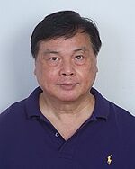
JOHN H LAU, Unimicron Technology Corporation, with more than 40 years of R&D and manufacturing experience in semiconductor packaging and SMT assembly, has published more than 510 peer-reviewed papers, 40 issued and pending US patents, and 22 textbooks on, e.g., Reliability of RoHS compliant 2D & 3D IC Interconnects (McGraw-Hill, 2011), Through-Silicon Via (TSV) for 3D Integration (McGraw-Hill, 2013), 3D IC Integration and Packaging (McGraw-Hill, 2016), and Assembly and Reliability of Lead-Free Solder Joints (Springer, 2020). John is an elected IEEE fellow, IMAPS Fellow, and ASME Fellow and has been actively participating in industry/academy/society meetings/conferences to contribute, learn, and share.
PDC D - Additive Printed Flexible Hybrid Electronics
Content
The production, design, assembly, and accelerated testing of additively printed flexible hybrid electronics for use in several cutting-edge fields will be discussed in this course. We will talk about the manufacturing procedures for flexible hybrid electronics that are made additively. Flexible hybrid electronics creates opportunities for the creation of stretchable, flexible, and foldable form-factors in electronics applications, which are not yet conceivable with the usage of rigid electronics technology. Flexible electronics may experience strain magnitudes in the range of 50 to 150 percent when used normally. When compared to rigid electronics, the integration methods and semiconductor package layouts for flexible hybrid electronics might be very different. Thin-chip integration, flexible encapsulation, compliant interconnects, and stretchable inks for metallization traces are all necessary for the production of thin electronic structures. It is now feasible to use a multitude of additive manufacturing techniques for the production and assembly of flexible hybrid electronics. In order to develop robust process parameters that will enable acceptable levels of yields in high-volume manufacturing, processes for handling, pick-and-place operations of thin silicon, and compliant interposers through interconnection processes like reflow, call for an understanding of the deformation and warpage processes. Flexible electronics may also require different testing, validation, and quality assurance procedures to assure reliability and survivability under exposure to prolonged harsh environmental working conditions
Instructor

PRADEEP LALL, Auburn University, Auburn, Alabama, United States, is the John and Anne MacFarlane Endowed Distinguished Professor in the Department of Mechanical Engineering with a courtesy joint appointment in both the Department of Electrical and Computer Engineering and in the Department of Finance. He serves on the technical council of NextFlex Manufacturing Institute and is academic co-lead of NextFlex’s Asset Monitoring Technical Working Group. He is the Director of the NSF Center for Advanced Vehicle and Extreme Environment Electronics at Auburn University. He is author and co-author of 2-books, 14 book chapters, and over 800 journal and conference papers in the field of electronics reliability, safety, energy efficiency, and survivability. Dr. Lall is a fellow of the ASME, fellow of the IEEE, a Fellow of NextFlex Manufacturing Institute, and a Fellow of the Alabama Academy of Science. He is recipient of the IEEE Region-3 Biedenbach Outstanding Engineering Educator Award, Auburn Research and Economic Development Advisory Board Award for Advancement of Research and Scholarship Achievement, IEEE Sustained Outstanding Technical Contributions Award, National Science Foundation’s Alex Schwarzkopf Prize for Technology Innovation, Alabama Academy of Science’s Wright A. Gardner Award, IEEE Exceptional Technical Achievement Award, ASME-EPPD Applied Mechanics Award, SMTA’s Member of Technical Distinction Award, Auburn University’s Creative Research and Scholarship Award, SEC Faculty Achievement Award, Samuel Ginn College of Engineering Senior Faculty Research Award, 3-Motorola Outstanding Innovation Awards, 5-Motorola Engineering Awards, and over 40-Best-Paper Awards at national and international conferences. Dr. Lall has served in several distinguished roles at national and international levels including serving as member of National Academies Committee on Electronic Vehicle Controls, Member of the IEEE Reliability Society AdCom, IEEE Reliability Society Representative on the IEEE-USA Government Relations Council for R&D Policy, Chair of Congress Steering Committee for the ASME Congress, Member of the technical committee of the European Simulation Conference EuroSIME, Associate Editor for the IEEE Access Journal, and Associate Editor for the IEEE Transactions on Components and Packaging Technologies. Dr. Lall is the founding faculty advisor for the SMTA student chapter at Auburn University and member of the editorial advisory board for SMTA Journal. He received the M.S. and Ph.D. degrees in Mechanical Engineering from the University of Maryland and the M.B.A. from the Kellogg School of Management at Northwestern University.Pradeep Lall is the John and Anne MacFarlane Endowed Distinguished Professor in the Department of Mechanical Engineering with a courtesy joint appointment in both the Department of Electrical and Computer Engineering and in the Department of Finance. He serves on the technical council of NextFlex Manufacturing Institute and is academic co-lead of NextFlex’s Asset Monitoring Technical Working Group. He is the Director of the NSF Center for Advanced Vehicle and Extreme Environment Electronics at Auburn University. He is author and co-author of 2-books, 14 book chapters, and over 800 journal and conference papers in the field of electronics reliability, safety, energy efficiency, and survivability. Dr. Lall is a fellow of the ASME, fellow of the IEEE, a Fellow of NextFlex Manufacturing Institute, and a Fellow of the Alabama Academy of Science. He is recipient of the IEEE Region-3 Biedenbach Outstanding Engineering Educator Award, Auburn Research and Economic Development Advisory Board Award for Advancement of Research and Scholarship Achievement, IEEE Sustained Outstanding Technical Contributions Award, National Science Foundation’s Alex Schwarzkopf Prize for Technology Innovation, Alabama Academy of Science’s Wright A. Gardner Award, IEEE Exceptional Technical Achievement Award, ASME-EPPD Applied Mechanics Award, SMTA’s Member of Technical Distinction Award, Auburn University’s Creative Research and Scholarship Award, SEC Faculty Achievement Award, Samuel Ginn College of Engineering Senior Faculty Research Award, 3-Motorola Outstanding Innovation Awards, 5-Motorola Engineering Awards, and over 40-Best-Paper Awards at national and international conferences. Dr. Lall has served in several distinguished roles at national and international levels including serving as member of National Academies Committee on Electronic Vehicle Controls, Member of the IEEE Reliability Society AdCom, IEEE Reliability Society Representative on the IEEE-USA Government Relations Council for R&D Policy, Chair of Congress Steering Committee for the ASME Congress, Member of the technical committee of the European Simulation Conference EuroSIME, Associate Editor for the IEEE Access Journal, and Associate Editor for the IEEE Transactions on Components and Packaging Technologies. Dr. Lall is the founding faculty advisor for the SMTA student chapter at Auburn University and member of the editorial advisory board for SMTA Journal. He received the M.S. and Ph.D. degrees in Mechanical Engineering from the University of Maryland and the M.B.A. from the Kellogg School of Management at Northwestern University.