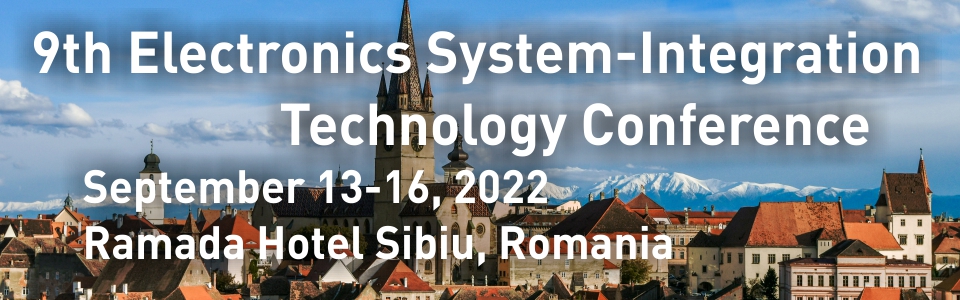


Keynote Presentations
Keynote 1 - Advanced Heterogeneous Integration Technology - A Key Enabler for Electronic Systems
Rolf Aschenbrenner, Fraunhofer Institute for Reliability and Microintegration, Berlin, Germany
The semiconductor industry is facing a new era in which device scaling and cost reduction will no longer continue on the path followed for the past few decades. The integration of more transistors into a monolithic IC is becoming more difficult and expensive at each node. Semiconductor companies are now looking for technological solutions to bridge the gap and improve cost performance, while at the same time adding more functionality through integration.
An attractive solution is heterogeneous integration (HI), that uses advanced packaging technologies to integrate devices, which can be designed and manufactured separately with the most suitable process technology and in the most optimized way. The package is also the ideal HI platform because it provides short connections, power efficient arrangement and high bandwidth between components in a compact form factor.
For example, with heterogeneous integration one can bring multiple chips (or chiplets) together into a single package. It elevates a conceptually similar multi-chip module to the next level by leveraging advanced wafer- or panel level manufacturing technologies.
This presentation will describe the value of advanced packaging as an HI platform. Key features in leading edge 2D and 3D technologies, such as wafer and panel level technologies will be described and new package developments from SoC to chiplet architecture will be presented. Challenges and opportunities in developing robust advanced package architectures will be discussed.
Rolf Aschenbrenner received the B. S. degree in mechanical engineering from the University for Applied Science, Gießen, Germany, in 1986 and the M.S. degree in physics from the University of Gießen, Germany, in 1991. From 1991 to 1992 he has worked at the University of Gießen and in 1993, he joined the Research Center for Microperipheric Technologies at the Technical University of Berlin. Since March 1994 he has been employed at the Fraunhofer Institute for Reliability and Microintegration Berlin (IZM) where he is presently the Deputy Director and Head of the Department System Integration and lnterconnection Technologies.
He received the iNEMI International Recognition Award in 2005, the CPMT David Feldman Outstanding Contribution Award 2013 and the European Semi Award 2016 .
As a member of the IEEE EPS Society Board of Governors Rolf Aschenbrenner has worked as a European representative on the Conference Advisory Board Committee, and has played an active role in the globalization of IEEE EPS in terms of membership and chapter development. He served as IEEE EPS Vice President, Technical and IEEE EPS Vice President, Conferences. From January 2010 until December 2011 he was IEEE EPS President and in 2012 he became IEEE Fellow.
Keynote 2 - Continental. Shaping the Future of Mobility
Sonok Rivetto, Continental Sibiu, Romania
Continental develops pioneering technologies and services for sustainable and connected mobility of people and their goods, having over 190.000 employees worldwide. Given the automotive field we are activating in, electronics systems play a fundamental role in our day-to-day R&D and manufacturing activities. In Sibiu we manufacture annually approximately 33 million electronic control units. The products developed, tested and manufactured here include intelligent braking systems, driving assist systems or connectivity systems. In present, Continental Sibiu has approximately 4000 employees. Together, they combine their knowledge in software and hardware development, design and simulation experience, innovation in artificial intelligence, big data and production processes.
In addition to trendsetting technologies such as automated and autonomous driving, smart infotainment and holistic connectivity, several very fundamental trends are influencing the automotive sector, such as digitalization, sustainability and efficiency. To master all these dimensions and stay ahead of the curve we rely on our talented #PeopleOfContinental. But new ideas need room to grow so at Continental we do our best to continuously develop our employees and offer a qualitative and inspirational working environment that empower our people to shape the future of mobility. Also, we build strong partnerships with the academia, investing in improving the technical skills of pupils and students – our future engineers.
Sonok Rivetto, the new General Manager of Continental Sibiu, is an American citizen, born in South Korea, coming to Sibiu after 18 years of experience in the Continental group. Over the years, she has held several positions at Seguin, Texas, as well as other Continental locations around the world.
With a Bachelor of Science in Mechanical Engineering and Master of Business Administration, Sonok has built a successful career at Continental. She learned about the company as a student participating in an externship program and joined right after the graduation from the university. Sonok has taken over various responsibilities in the area of production, business and general management.
Keynote 3-1 - Sustainable Lithium-Ion Batteries
Ulla Lassi, Applied Chemistry and Process Chemistry, University of Oulu, Finland
The demand for lithium-ion batteries is growing rapidly due to the increasing popularity of electric vehicles, portable devices, and energy storage from renewable energy sources, particularly household electricity generated by wind power and solar cells. This means increasing battery capacity need, and new Gigafactories are being built in Europe. Further, several investment plans for the manufacture of batteries and battery chemicals have also been published. The growing need for batteries will significantly increase the need for both primary battery minerals and recycled materials. However, these secondary materials alone are not enough to cover even the current need for battery materials. Therefore, we need responsible mining and sustainable battery mineral processing. Discussions on sustainability raise often the role of cobalt in battery metals, its availability and, in particular, the ethical aspects related to cobalt processing chain. Cobalt has been paid too much attention in this regard, as already in existing lithium-ion batteries; the use of cobalt is quite low and will decrease significantly with new NMC chemistries and even completely cobalt-free chemistries. In addition, cobalt can be efficiently recycled from lithium-ion batteries, as can nickel. In addition to battery metals, the focus should also be on current cell manufacturing processes, which typically use toxic solvents and fluorinated binders or electrolyte salts. These compounds pose challenges not only from the viewpoint of battery cells recycling but also from the point of view of ecology and safety. In our own research, we have recently focused on new cell manufacturing methods. At the same time, we have been able to replace e.g. harmful NMP solvent and binders with new material choices without compromising the performance of the battery cell itself. Such a greener cell manufacturing technology would also like to be transferred to the production of more and more battery factories in the short term.
Ullas Lassi: Doctor of Technology, in 2003. Since 2006, Professor in Applied Chemistry and Process Chemistry, University of Oulu, Faculty of Technology. Currently also the Head of Research Unit of Sustainable Chemistry (51 employers), at the university of Oulu. Her research areas involve inorganic material chemistry in industrial applications, esp. heterogeneous catalysis in biomass conversion and wastewater treatment as well as lithium-ion battery chemicals. She has over 140 peerly-reviewed scientific publications. As a professor, she has supervised 20 Ph.D. theses and more than 100 M.Sc. theses. She has been principal investigator of 30 research projects. Professor Lassi is also an active member in several scientific and educational societies and committees. She has several positions of trust.
Keynote 3-2 - Reliability in Harsh Automotive Environments
Pradeep Lall, Auburn University, Auburn, Alabama, United States
Automotive platforms are increasingly using electronics for a range of mission-critical and safety-critical functions, including guidance, navigation, control, charging, sensing, and operator contact. Hybrid electric vehicles and fully-electric vehicles have been included into automotive platforms over the past twenty years. The majority of the electronics are found in the trunk or under the hood of the car, where temperatures and vibration levels are much higher than in consumer or office applications. Electronics in the automobile underhood may be exposed to sustained high temperatures of 125–150°C for prolonged periods of time throughout the vehicle's useful life. Electronics used in automobiles are divided into four grades by the Automotive Electronics Council (AEC): grade-0, grade-1, grade-2, and grade-3. With anticipated power temperature cycling ranging from -40°C to +150°C for 1000 cycles and ambient temperature cycling ranging from -55°C to +150°C for 2000 cycles, Grade-0 components have the strictest requirements among the four grade categories. Additionally, it is expected that grade-0 components can withstand 175°C high temperature storage for 1000 hours. The field of packaging applications has developed further with the development of novel package structures, enabling powerful computing on mobile car platforms. A tighter integration of electronics sensing and processing into the structural features of the vehicle is now possible due to the development of new materials and integration technologies. The real-time context of the automotive platform imposes a number of restrictions on the ability to provide advanced functionality.
Pradeep Lall is the John and Anne MacFarlane Endowed Distinguished Professor in the Department of Mechanical Engineering with a courtesy joint appointment in both the Department of Electrical and Computer Engineering and in the Department of Finance. He serves on the technical council of NextFlex Manufacturing Institute and is academic co-lead of NextFlex’s Asset Monitoring Technical Working Group. He is the Director of the NSF Center for Advanced Vehicle and Extreme Environment Electronics at Auburn University. He is author and co-author of 2-books, 14 book chapters, and over 800 journal and conference papers in the field of electronics reliability, safety, energy efficiency, and survivability. Dr. Lall is a fellow of the ASME, fellow of the IEEE, a Fellow of NextFlex Manufacturing Institute, and a Fellow of the Alabama Academy of Science. He is recipient of the IEEE Region-3 Biedenbach Outstanding Engineering Educator Award, Auburn Research and Economic Development Advisory Board Award for Advancement of Research and Scholarship Achievement, IEEE Sustained Outstanding Technical Contributions Award, National Science Foundation’s Alex Schwarzkopf Prize for Technology Innovation, Alabama Academy of Science’s Wright A. Gardner Award, IEEE Exceptional Technical Achievement Award, ASME-EPPD Applied Mechanics Award, SMTA’s Member of Technical Distinction Award, Auburn University’s Creative Research and Scholarship Award, SEC Faculty Achievement Award, Samuel Ginn College of Engineering Senior Faculty Research Award, 3-Motorola Outstanding Innovation Awards, 5-Motorola Engineering Awards, and over 40-Best-Paper Awards at national and international conferences. Dr. Lall has served in several distinguished roles at national and international levels including serving as member of National Academies Committee on Electronic Vehicle Controls, Member of the IEEE Reliability Society AdCom, IEEE Reliability Society Representative on the IEEE-USA Government Relations Council for R&D Policy, Chair of Congress Steering Committee for the ASME Congress, Member of the technical committee of the European Simulation Conference EuroSIME, Associate Editor for the IEEE Access Journal, and Associate Editor for the IEEE Transactions on Components and Packaging Technologies. Dr. Lall is the founding faculty advisor for the SMTA student chapter at Auburn University and member of the editorial advisory board for SMTA Journal. He received the M.S. and Ph.D. degrees in Mechanical Engineering from the University of Maryland and the M.B.A. from the Kellogg School of Management at Northwestern University.
Keynote 3-3 - CNF-MIM Technology, Enabling the Worlds Thinnest Capacitor
Maria Bylund, Smoltek AB, Gothenburg, Sweden
This keynote will present a novel technology (CNF-MIM) combining Carbon Nanofiber (CNF) materials and MIM (metal-insulator-metal)-like technology, enabling capacitors with total thickness lower than 40 µm suitable for use in future miniaturized electronics. The ultra-thin and discrete CNF-MIM capacitors have been manufactured and characterized on several substrates, showing excellent electrical properties such as high capacitance density of several hundreds of nF/mm2 , ESR (equivalent series resistance) in the mOhm range, low ESL (equivalent series inductance) on the order of 10 pH thus being promising for a multitude of applications within the semiconductor industry. To assess the long-term durability, CNF-MIM capacitors have also been subjected to prolonged exposure to high temperature and constant voltage bias environments following a HTS (high temperature storage) and BTS (biased temperature stress) standard. The CNF-MIM capacitor show initial robustness against degradation in these scenarios.
Maria Bylund received her B.Sc. degree of Applied Mechanics and her Master’s degree of Materials Science and Engineering from the Chalmers University of Technology in 2009 and 2011, respectively. She worked as test engineer at SKF Sverige AB; as CAE Engineer and then as Project Assistant at the Chalmers University of Technology, all in Gothenburg, Sweden. Since 2018, she has been working as R&D Engineer at Smoltek AB, which company has focused towards the area of nanostructure technology. They are – among other things – working in the field of nanofabrication towards the semiconductor industry. Her tasks are to plan, perform and thoroughly document and evaluate projects within this area, using advanced equipment and methods common to the nanofabrication area as well as advanced analysis methods. She commonly does growth of carbon nanofibers (CNFs) in a PECVD (Plasma Enhanced Chemical Vapor Deposition) system, photolithography, different kinds of metal depositions such as sputtering, physical vapor deposition (PVD) and atomic layer deposition (ALD) and other processing can include e.g. wet and dry etching, heat treatments and such. Testing and confirming of processing and properties in between process steps as well as after completed production is paramount to the production. Electrical properties are evaluated using a Parameter Analyzer Probing Station and a Vector Network Analyzer (VNA) connected to a probing station. Visual evaluation is mainly done with the help of optical light microscopy and Scanning Electron Microscopy (SEM). A great portion of her work is performed at Myfab, a Nano fabrication facility located at Chalmers University of Technology. This laboratory is a cleanroom, which requires special training to access and individual personal licenses to operate the machines.
Keynote 3-4 - Nanomaterial-Enabled Soft Electronics
Yong Zhu, Andrew A. Adams Distinguished Professor, North Carolina State University (NCSU), USA
Highly sensitive wearable sensors that can be conformably attached to human skin or integrated with textiles to monitor the physiological parameters of human body or the surrounding environment have garnered tremendous interest. Owing to the large surface area and outstanding material properties, nanomaterials are promising building blocks for wearable sensors. In this lecture I will start with a brief overview of the recent advances in the nanomaterial-enabled soft electronics (e.g., flexible, stretchable, and wearable sensors and soft robotics). Integration of multiple sensors for multimodal sensing and integration with other components into wearable systems will be summarized. Then I will present the array of wearable sensors developed in my group using silver nanowire (AgNW) composites including strain/pressure sensors, hydration sensors, temperature sensors, antennas and etc. AgNW composites offer outstanding combination of high conductivity and high stretchability. I will highlight a critical issue for developing AgNW-based stretchable devices – scalable nanomanufacturing. Electronic waste has become a pressing issue that poses a threat to health and environment. Here I will propose a recycling approach to address the issue using AgNWs as an example. I will conclude my talk with some recent work extending from wearable sensors for human health to wearable plant sensors and soft robotics.
Prof. Yong Zhu is the Andrew A. Adams Distinguished Professor in the Department of Mechanical and Aerospace Engineering, with affiliated appointments in the Departments of Materials Science and Engineering and Biomedical Engineering, at North Carolina State University (NCSU). His group conducts research at the intersection of solid mechanics and micro/nano-technology, including nanomechanics, interfacial mechanics, micro/nano-electromechanical systems, and nanomaterial-enabled stretchable electronics.
Keynote 3-5 - Advanced Packaging: Enabling a New Generation of Silicon Systems
Mark Gerber, Sr. Director, Engineering & Technical Marketing, ASE, Inc.
Demand for new efficiencies in the semiconductor design and manufacturing process is propelling the increasingly vital role of packaging to deliver on requirements related to miniaturization, power and performance. During his presentation, Mark will explore heterogeneous integration and chiplet innovation, and describe how advanced packaging technologies are enabling highly complex system integration, which is required to create a smarter and more sustainable world for generations to come.
Mark Gerber heads engineering and technical marketing in his capacity as Senior Director at ASE. With over twenty-five years’ experience in the semiconductor industry, Mark previously held management and engineering roles at Texas Instruments, Motorola, and Maxim Integrated in various areas of design, manufacturing, and assembly with an emphasis on the development of new technologies and processes. Mark serves on multiple committees for IEEE and IMAPS and is an IMAPS Fellow. He holds a Bachelor’s degree in mechanical engineering from Texas A&M University, has written over 20 papers and publications, and holds 36 semiconductor packaging related patents.
Keynote 4 - Reliability Testing and Design for Reliability of Lead-Free Solder Joints
John H Lau, Unimicron Technology Corporation
The recent advances and trends of lead-free solder joint reliability are presented in this study. Emphasis is placed on the design for reliability (DFR) and reliability testing and data analysis. For DFR: (a) the Norton power creep constitutive equations and examples for Au20Sn, Sn58Bi, Sn3.8Ag0.7Cu, and Sn3.8Ag0.7Cu0.03Ce, (b) the Wises two power creep constitutive equations and examples for Sn3.5Ag and Sn4Ag0.5Cu, (c) the Garofalo hyperbolic sine creep constitutive equations and examples for Sn3.5Ag, Sn3Ag0.5Cu, Sn3.9Ag0.6Cu, Sn3.8Ag0.7Cu, Sn3.5Ag0.5Cu, and Sn3.5Ag0.75Cu, Sn4Ag0.5Cu, Sn(3.5- 3.9)Ag(0.5-0.8)Cu, 100In, Sn52In, Sn3.8Ag0.7Cu0.03Ce, and Au20Sn, and (d) the Anand viscoplasticity constitutive equations and examples for Sn3.5Ag, Sn3Ag0.5Cu, Sn3.8Ag0.7Cu, Sn3.8Ag0.7CuCe, Sn3.8Ag0.7CuAl, Au20Sn, Sn3.5Ag with temperature and strain rate-dependent parameters, and Sn1Ag0.5Cu, Sn2Ag0.5Cu, Sn3Ag0.5Cu, and Sn4Ag0.5Cu after extreme aging will be discussed. For reliability testing and data analysis: (a) the Weibull and lognormal life distributions for lead-free solder joints under thermal-cycling and drop tests, (b) the true Weibull slope, true characteristic life, and true mean life, and (c) the linear acceleration factors for various lead-free solder alloys based on: (i) frequency and maximum temperature, (ii) dwell time and maximum temperature, and (iii) frequency and mean temperature will be presented. Some recommendations will also be provided
John H Lau, with more than 40 years of R&D and manufacturing experience in semiconductor packaging and SMT assembly, has published more than 510 peer-reviewed papers, 40 issued and pending US patents, and 22 textbooks on, e.g., Reliability of RoHS compliant 2D & 3D IC Interconnects (McGraw-Hill, 2011), Through-Silicon Via (TSV) for 3D Integration (McGraw-Hill, 2013), 3D IC Integration and Packaging (McGraw-Hill, 2016), and Assembly and Reliability of Lead-Free Solder Joints (Springer, 2020). John is an elected IEEE fellow, IMAPS Fellow, and ASME Fellow and has been actively participating in industry/academy/society meetings/conferences to contribute, learn, and share.
Keynote 5 - About the mission of Siemens Digital Industries Software
Oren Manor, Siemens Digital Industries Software, Tel Aviv, Israel
Siemens Digital Industries Software is driving transformation to enable a digital enterprise where engineering, manufacturing and electronics design meet tomorrow. Our solutions help companies of all sizes create and leverage digital twins that provide organizations with new insights, opportunities and levels of automation to drive innovation. For more information on Siemens Digital Industries Software products and services, visit sw.siemens.com.
Oren Manor holds a B.Sc. in Computer Science and Economics from Tel-Aviv University. He has been the Siemens Opcenter Core Business Director at Siemens Digital Industries Software since October 2021, where he manages the overall business strategy for the Digital Manufacturing portfolio for the Medical, Electronics and Semiconductors Industries. Before this he was Electronics Manufacturing Business Director at Mentor Graphics’ Valor Division. Oren Manor joined the Valor Division of Mentor Graphics in 2012 and served in a number of key business positions including Partner Management and Manufacturing Engineering Business Development. He previously served as VP of Sales and Marketing at Signature-IT, a software company providing data management solutions for industrial companies, and held senior sales and marketing positions at Jungo – a NDS company. After living in Stockholm, London, Philadelphia and Chicago, Oren resides in Tel Aviv. He is passionate about technology and an evangelist for automating electronics manufacturing; expert in Electronics, Medical, Semiconductor and discrete manufacturing; frequent speaker at leading industry and Siemens Software events. He has extensive Business Development experience in building comprehensive go-to-market strategies for Enterprise and B2B software applications.